

Diana Meneses-Gustin (Photo by Jean Andrews/Ohio University)
Physicists from Ohio University and the Federal University of Sao Carlos in Brazil have partnered to unravel the atomic mechanism that can be used to create nanometer scale and fully reversible electronic circuits on two-dimensional materials.
This work was led by doctoral student Diana Meneses-Gustin and is part of an ongoing collaboration with the research group of Professor Victor Lopez-Richards at UFSCar, Meneses-Gustin visited OHIO and worked in the group of Dr. Sergio Ulloa as part of her doctoral studies. Ulloa is a professor in Physics and Astronomy, and member of OHIO’s Nanoscale & Quantum Phenomena Institute.
Their findings “Photomodulation of transport in monolayer dichalcogenides”, were published as a Rapid Communication in the journal Physical Review B, identified for their timeliness and significance to the field.

Dr. Sergio Ulloa (Photo by Jean Andrews/Ohio University)
“Some molecules change conformation when absorbing light, modifying their shape and associated charge distribution,” Ulloa said. “An example of this behavior is the azobenzene molecule—two carbon rings connected by a nitrogen “hinge”—which in the dark adopts a linear configuration where the nitrogen-nitrogen hinge is open and places the two rings on the same plane, parallel, and head-to-toe of each other.”
When illuminated with ultraviolet light, the nitrogen hinge partially closes and the two rings shift to being perpendicular to one another, in an L configuration. “We also know that the L configuration relaxes by itself to the planar arrangement or can be stimulated to do so when illuminated with white light. And most importantly, these changes are fully reversible,” Ulloa emphasized.
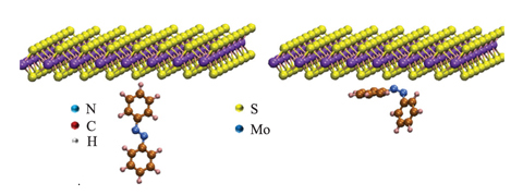
Molecule in two different conformations near a two-dimensional material
The OHIO-Brazil collaboration shows theoretically that such conformational change can also be used to produce changes in the electronic environment of a layer material in close proximity.
Using state-of-the-art atomistic calculations of the structure, as well as electronic scattering theory, the OHIO-Brazil collaboration identified the reason for such strong effects on the monolayer nearby. As the nitrogen-hinge closes, it can locally change the electrostatic potential experienced by the electrons in the monolayer. When that happens, the electronic motion on the layer is locally perturbed, which can affect various experimental results.
“This behavior demonstrates the possibility for the reversible writing or erasing of nanoscale conducting paths or barriers on a layer,” said Ulloa. “Using light to open or close electronic paths is unique to such hybrid materials, and a large variety of combinations can be formed.”
Ulloa’s research on this topic was supported by the National Science Foundation.
Abstract: Surface functionalization emerges as an alternative pathway for electronic structure engineering in two-dimensional (2D) systems. We explore a hybrid heterostructure built from a 2D transition-metal dichalcogenide atop a layer of photochromic self-assembled azobenzene molecules. This setup can modify carrier transport through the 2D nanosheet by an effective photoactived gating control, achieved through trans to cis isomerization of the azobenzene in close contact with the 2D nanosheet. We show theoretically that this behavior can be ascribed to a tunable gating mechanism. We use a combination of atomistic calculations of the local effective potential profile with simulations of the electron scattering by such potential in a massive Dirac Hamiltonian formalism. We find that different isomers induce a local perturbation with drastically different features that explain well the experimental behavior.


Comments