
Analysis of molybdenum disulfide film growth.
By Raymond Humienny
NQPI editorial intern
Imagine growing the materials you need for a device right onto the metal contacts in a circuit.
Dr. Eric Stinaff, Professor of Physics & Astronomy and Director of the Nanoscale and Quantum Phenomena Institute at Ohio University, has already filed for a provisional patent that exploits this procedure.
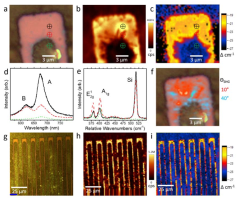
Stinaff and Dr. Martin Kordesch, fellow Physics & Astronomy professor and NQPI member, successfully demonstrated how a chemical vapor deposition (CVD) technique can be used to grow monolayer transition metal dichalcogenides (TMDs) on a molybdenum pattern. The paper can be viewed in Advanced Materials Interfaces.
“The metal (molybdenum) acts … as a seed and a catalyst,” Stinaff said.
The application of Stinaff’s technique can potentially simplify manufacturing of optoelectronic devices such as LEDs and solar cells. Instead of performing extensive lithography to fit a metallic pattern to pre-grown TMDs, Stinaff begins by producing the molybdenum patterns to catalyze TMD growth.
TMDs are compounds typically referred to as MX2, where M symbolizes a transition metal and X represents the surrounding chalcogen atoms. The compound of choice for Stinaff was molybdenum disulfide (MoS2), a monolayer semiconductor. Since this TMD only consists of a single layer, MoS2 has a negligible volume and many other properties that are useful for optoelectronic devices.
CVD involves treating a metallic oxide powder with sulfur residue through intensive heating in a furnace. Stinaff’s CVD procedure includes molybdenum trioxide (MoO3) and sulfur powder to grow MoS2 on a molybdenum pattern sitting atop a substrate. A flow of argon is used to treat the MoO3 with the sulfur residue, decomposing the MoO3.
“The molybdenum powder will essentially vaporize and … interact with the sulfur,” Stinaff said. “What’s happening in that (reaction is) you’re forming MoS2 constituents, or atoms, and they’ll meet up with other ones and start to build the material.”
Moreover, directed MoS2 growth provides new research directions. When used in CVD, Stinaff said that metals such as titanium produce little to no MoS2 growth and might be useful for designing complex patterns. Additionally, Stinaff has observed how other TMDs interact with MoS2 growth and conductivity. Tungsten disulfide (WS2) is another TMD that Stinaff has used on molybdenum to create hetero-structures of WS2 and MoS2 layered material.
With future research focused on determining the electrical properties of test devices, Stinaff said the team hopes to eventually turn this project into an industrial method.
“What I think is really important about the work that we’re doing is it provides a very simple way to make devices using these materials,” Stinaff said.


Comments