
(L-R) Physicists Diego Mastrogiuseppe, Sergio Ulloa, and Nancy Sandler
By Jean Andrews
Physics & Astronomy
Diego Mastrogiuseppe, a postdoctoral researcher in the Department of Physics & Astronomy, and faculty members Dr. Nancy Sandler and Dr. Sergio Ulloa, have discovered a new way to control the interaction of magnetic impurities at the nanoscale level.
The article describing their work has been published in Physical Review B, a condensed matter and materials physics journal of the American Physical Society. The APS designated the researchers’ discovery as meriting a Rapid Communication, placing it ahead of articles similar in subject matter.
“We found that magnetic impurities at the nanoscale prefer twisting in new two-dimensional materials. This discovery suggests a number of experiments that include direct imaging using spin polarized scanning tunneling microscopy, a technique used by Arthur Smith, our colleague and fellow member of the Nanoscale & Quantum Phenomena Institute,” explained Sandler.
The researchers studied how the interaction between two magnetic atoms (impurities) is affected by the electron charge density in recently developed materials.
They demonstrated that as the charge carrier concentration varies in a monolayer of a molybdenum disulfide crystal, the interaction between two magnetic atoms (analogous to small magnets) deposited on its surface, may be controlled to favor the usual parallel-antiparallel configuration, or instead tune it to favor equilibrium twisting orientations.
“Once such carrier control is set in place, one could use this effect to externally control the configurations of ensembles of magnetic impurities, possibly transferring information over distances,” Mastrogiuseppe explained.
“This may open the door to innovative data storage and manipulation schemes that utilize the relative orientation of magnetic impurities in these two-dimensional materials.”
How It Works: Using Graphene’s ‘Chicken Wire’ to Build New Devices
Researchers are investigating a variety of novel two-dimensional materials where crystals are analyzed at the atomic level. Graphene is one of the most prominent materials, which is made of a monoatomic layer of carbon atoms arranged in a honeycomb arrangement (similar to that seen in chicken wire.)
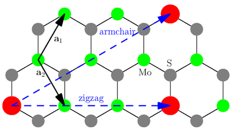
The figure represents a “chicken wire” lattice characteristic of a tri-layer MoS_2 crystal. Green circles represent molybdenum atoms while grey ones are sulfur atoms. Magnetic impurities are shown as red dots. Blue arrows indicate the distance between any two of them. Each impurity possesses a net magnetic moment that can be aligned with the others in a parallel/antiparallel or twisted configuration depending on the charge density in the MoS2 crystal.
A family of compounds known as transition metal dichalcogenides, close relatives to graphene, is attracting a great deal of attention. These materials span a number of different electronic properties and are promising candidates for a new generation of devices in the realm of low-dimensional systems. One prototypical example of these compounds is molybdenum disulfide (MoS2), where the molybdenum atomic layer is literally sandwiched between two sulfur atomic layers. This tri-atomic material is a semiconductor with unusual properties and extremely thin.
Electrons moving in this material experience their interaction with the underlying crystal as if they were relativistic objects. Their spin (a measure of their magnetic nature) gets entangled with their momentum (a measure of their velocity), effect known as the ‘spin-orbit interaction’. Because the electron’s momentum is easily manipulated with electric fields (i.e. voltages) the spin-orbit interaction makes it possible to manipulate the spin of the electrons by electrical means. This interaction is a fundamental ingredient in spintronics, an emerging field involving the detection and manipulation of electron spin at the nanoscale level. Spintronics offers a new paradigm in the search to develop faster and more efficient electronic devices.
As two magnetic impurities are separately deposited in these trilayer dichalcogenides, they acknowledge each other’s presence indirectly, via the moving electrons of the host material. This process is known as the RKKY or Ruderman-Kittel-Kasuya-Yosida interaction. In conventional metals, the RKKY interaction oscillates with the separation between the two magnetic impurities, rendering the magnetic moments of both impurities pointing along the same direction or opposite directions depending on the distance between them.
“In dichalcogenide materials however, the presence of spin-orbit interaction can produce a twisted magnetic configuration, so that the relative alignment of the impurities is no longer parallel or antiparallel,” said Mastrogiuseppe.
A magnetic impurity contains the minimal representation of a bit, the elementary unit of information used in electronics nowadays. The direction of its magnetic moment (up or down) translates into the standard 0 and 1 used to record information. Thus, a bunch of magnetic moments allows one to write a string of 0 and 1 with their directions aligned or anti-aligned. The advantage of producing configurations where the directions may not be all in the same plane but ‘twisted’ is that the amount of information encoded is significantly bigger. Devices built on these principles have the potential not only of storing more information but of performing larger calculations much faster than classical devices.
Ulloa is optimistic that the future is bright for new and improved devices. “Studying the physics of electronic spins in materials is not only exciting and challenging physics, but it will give rise to a whole new area of device applications in the near future!”


Comments